Hemt Pr
Galliumnitrid Wikipedia

Hey Say Jump おしゃれまとめの人気アイデア Pinterest Mo

Moscap And Hemt Process Flows A Moscap Process Flow N Gan Substrate Download Scientific Diagram
Www Theses Fr 17limo0084 Pdf

Device Characteristics Of Enhancement Mode Double Heterostructure Dh Hemt With Boron Doped Gan Gate Cap Layer For Full Bridge Inverter Circuit Mohanbabu 18 International Journal Of Numerical Modelling Electronic Networks Devices And

Flk017xp Datasheet Eudyna Devices Datasheetspdf Com
This Time incよりCAMPINOXのデジカモショルダーバッグがhouyhnhnmjp読者プレゼントになりました。 詳しくはhouyhnhnmjpをご確認ください。(締め切り12年5月16日).

Hemt pr. HEMT PR, 東京都 渋谷区 642 likes HEMT PRは、ファッションブランド、ファッションメーカーのPR及び ブランディングを行うPRオフィスです。 クリエイターの情熱を消費者へ伝える創造性豊かなプロモーション、 展示会やイベントに向けた構築的な販促企画を提案します。. Teledyne’s TDG650E60 GaN Power HEMT boasts an extremely small form factor and leverages the patented Island Technology® from GaN Systems This technology is a scalable, vertical charge dissipating system that gives the power transistor ultralow thermal losses, high power density, nocharge storage, and very high switching speeds. HEMT with HZO dielectric shows an enhanced DC output performance with an increase of 54% at the optimal working condition, which is indeed much higher than that of the HfO2 MOSHEMT (40%) And the HZO MOSHEMT exhibits a higher Ion/Ioff ratio of 106, an excellent subthreshold swing (SS) of 85 mV/decade, and a.
Our gallium nitride (GaN) HEMT epiwafer products are well known for their high breakdown voltage with low leakage current and excellent two dimensional electron gas (2DEG) characteristics The products are used worldwide by major cuttingedge semiconductor device companies. 12 AUTUMN & WINTER よりスタートのFAHBLE(ファーブル)がeyescreamjp、Houyhnhnm Blogで紹介されています。 普遍的であり先進的、機能性と将来性を意匠(デザイン)に表現し、洋服という媒体を介して、ただ着るのみでなく、日常生活が魅力的なエナジーに感じられるようなリアルクローズを. HEMT PRは、ファッションブランド、ファッションメーカーのPR及びブランディングを行うPRオフィスです。クリエイターの情熱を消費者へ伝える想像性豊かなプロモーション、展示会やイベントに向けた構築的な販促企画を提案します。 HEMT PR tel 東京都渋谷区渋谷1171 TOC第2ビル902.
12 AUTUMN & WINTER よりスタートのFAHBLE(ファーブル)がeyescreamjp、Houyhnhnm Blogで紹介されています。 普遍的であり先進的、機能性と将来性を意匠(デザイン)に表現し、洋服という媒体を介して、ただ着るのみでなく、日常生活が魅力的なエナジーに感じられるようなリアルクローズを. The epitaxial layers were grown on a 2in Si (111) substrate by MOCVD After the preparation of the epitaxial wafer, the normallyoff pGaN/AlGaN/GaN HEMT on a Si substrate was achieved by hydrogen plasma treatment The main structure of the epitaxial wafer includes a 1 µm GaN buffer layer, a 100 nm GaN channel layer, a 1 nm AlN spacer layer, an 18 nm undoped Al 02 Ga 08 N barrier layer. PR PR PR Sapphire Substrate Buffer GaN AlGaN ②Mask 02 –S/D Ø Sourceanddraincontactto AlGaN Ø Themetalmustbe depositedafteracompletely cleanprocesstoeliminate layersbetweenAlGaNand Metal A GaNonSapphire HEMT Process Flow Example ③Deposit S/D metal Ø Deposit ohmic contacts on top of AlGaN as source and drain Sapphire Substrate Buffer.
Output power of 100 mW was the pump source For PR measurements, a DC 3 V tungstenhalogen lamp was the whitelight source, and a HeNe laser (6328 nm) acted as the modulation light source of the HEMT sample Measurements of an InGaAs/GaAs gradedchannel HEMT have been carried out with this PL and PR system Optical Characterization of. Teledyne e2v HiRel ajoute deux nouveaux HEMT (transistors à haute mobilité électronique) de puissance GaN renforcés à sa gamme de produits haute puissance de 650 volts à la pointe du secteur. Copyright 19 hemt pr all rights reserved.
Teledyne e2v HiRel ajoute deux nouveaux HEMT (transistors à haute mobilité électronique) de puissance GaN renforcés à sa gamme de produits haute puissance de 650 volts à la pointe du secteur. MAISON ALTERNATIVE (HEMT PR) YOAK (HEMT PR) UNUSED la favola Nagasaki Film & Media Commission (JFC) The Former Hong Kong and Shanghai Bank Nagasaki Branch Museum Hotel Nagasaki Photo Shunya Arai Styling Lambda Takahashi Hair & Makeup Yusuke Morioka Model Etienne Marisa Edit Takuya Chiba Takayasu Yamada. Output power of 100 mW was the pump source For PR measurements, a DC 3 V tungstenhalogen lamp was the whitelight source, and a HeNe laser (6328 nm) acted as the modulation light source of the HEMT sample Measurements of an InGaAs/GaAs gradedchannel HEMT have been carried out with this PL and PR system Optical Characterization of.
The fabricated 1 μm long gate GaN HEMT, Pr 2 O 3 MISHEMT, and P 2 S 5 /(NH 4) 2 UVtreated Pr 2 O 3 MISHEMT were tested onwafer and the microwave power characteristics were evaluated using a loadpull system with automatic tuners, which simultaneously provides conjugatematched input and load impedances for the maximum output power The. For PL measurements of the HEMT device, a frequencydoubled NdYAG laser (532 nm) with average output power of 100mW was used as the pump source For PR measurements, a DC 3V tungsten halogen lamp was used as the whitelight source, and a HeNe laser (6328 nm) acted as the modulation light source of the HEMT sample. µm GaAs pHEMT is a pr actical tech nology of ch oice because it offers balan ced over all pe rforman ce for Kuba nd PA application s IV C ONCLUSION This pap er p resents the 3stage c.
Hemt Watches Buy Hemt Watches Store Online at Best Prices in India Shop Online for Watches Store Get Free Shipping and Home Delivery at Flipkartcom. Gallium Nitride (GaN) High Electron Mobility Transistor (HEMT) has significant advantages over traditional Si MOSFETs due to its lower gate charge and smaller output capacitance which lead to faster switching and lower losses Also, the absence of body diode in GaN allows zero reverse recovery thus making it viable in highfrequency power converters. Fujitsu Limited and Fujitsu Laboratories Ltd today announced the development of a new type of gallium nitride (GaN) based high electron mobility transistor (HEMT) that features a new structure ideal for use in amplifiers for microwave and millimeterwave transmissions, frequency ranges for which usage is expected to grow In a technological first, a novel transistor structure was developed.
PR PR PR Sapphire Substrate Buffer GaN AlGaN ②Mask 02 –S/D Ø Sourceanddraincontactto AlGaN Ø Themetalmustbe depositedafteracompletely cleanprocesstoeliminate layersbetweenAlGaNand Metal A GaNonSapphire HEMT Process Flow Example ③Deposit S/D metal Ø Deposit ohmic contacts on top of AlGaN as source and drain Sapphire Substrate Buffer. This study elucidates the praseodymium oxide (Pr 2 O 3)passivated AlGaN/GaN metal–oxide–semiconductor high electron mobility transistors (MOSHEMTs) with high dielectric constant, and with their AlGaN Schottky layers treated with P 2 S 5 /(NH 4) 2 S X ultraviolet (UV) illumination An electronbeam evaporated Pr 2 O 3 insulator is used, instead of traditional plasmaassisted chemical. Hemt prは、ファッションブランド、ファッションメーカーのpr及び ブランディングを行うprオフィスです。 クリエイターの情熱を消費者へ伝える創造性豊かなプロモーション、 展示会やイベントに向けた構築的な販売促進を提案します。.
The name HEMT stands for High Electron Mobility Transistor The device is a form of field effect transistor, FET, that utilises an unusual properly of a very narrow channel enabling it to operate at exceedingly high frequencies In addition to the very high frequency performance, the HEMT also offers a very attractive low noise performance. Fujitsu Limited and Fujitsu Laboratories Ltd today announced the development of a new type of gallium nitride (GaN) based high electron mobility transistor (HEMT) that features a new structure ideal for use in amplifiers for microwave and millimeterwave transmissions, frequency ranges for which usage is expected to grow In a technological first, a novel transistor structure was developed. µm GaAs pHEMT is a pr actical tech nology of ch oice because it offers balan ced over all pe rforman ce for Kuba nd PA application s IV C ONCLUSION This pap er p resents the 3stage c.
スニーカー¥25,000/ヨーク(hemt pr ) 掲載した商品はすべて税抜き価格になります。 「アエラスタイルマガジンVOL48 WINTER 」 より転載. GaN HEMT is a promising alternative of Si MOSFET for the highdensity power converter applications Due to their lower switching losses, GaN HEMT may lead to new horizons in the application area. Based on Equation 4, the third quadrant characteristic of GaN HEMT is derived and plotted in Figure 17 Compared with Si MOSFET’s body diode, GaN HEMTs have higher Vsd drop as Vth Vgs is usually higher than 07 V when the gate is off For instance, the commercial 650 V enhancementmode GaN device has a typical.
YOAK18 Spring & Summer CollectionがHOUYHNHNMで紹介されました。 一度フイナムでもご紹介した新鋭スニーカーブランドの〈ヨーク(YOAK)〉。“ジャケットやシャツに合わせる事を前提に作る” というブランド哲学に基づいたクリーンな装いが話題を呼び、いよいよ無視できない注目のブランドと. 279 Followers, 78 Following, 97 Posts See Instagram photos and videos from HEMT PR (@hemt_pr). The epitaxial layers were grown on a 2in Si (111) substrate by MOCVD After the preparation of the epitaxial wafer, the normallyoff pGaN/AlGaN/GaN HEMT on a Si substrate was achieved by hydrogen plasma treatment The main structure of the epitaxial wafer includes a 1 µm GaN buffer layer, a 100 nm GaN channel layer, a 1 nm AlN spacer layer, an 18 nm undoped Al 02 Ga 08 N barrier layer.
The integrated power GaNs have R DS(ON) of 150 mΩ and 650 V drain‑source breakdown voltage, while the high side of the embedded gate driver can be easily supplied by the integrated bootstrap diode The MASTERGAN1 features UVLO protection on both the lower and upper driving sections, preventing the power switches from operating in low efficiency or dangerous conditions, and the interlocking. Of all the tools in Veeco’s lineup, Veeco’s WaferStorm® is the workhorse for wet processing applications for RF device processes including metal liftoff (MLO) and photoresist (PR) strip applications MLO is critical for RF filter manufacturing as a costeffective alternative to etch processes that can damage underlying substrates. AlGaN/GaN HEMT s ar e pr omising ca ndidates f or next genera tion microwa ve power am pli ers and highvol tage switch es owing to their superior p roperties ,.
Bukht12 AUTUMN & WINTER COLLECTIONがeyescreamjpで公開されています。 デザイナー:橋本哲也 12 A/Wテーマ 「I leave it your imagination=あなたのご想像にお任せします」 今シーズンのブフトは“I leave it your. The HEMT is a newly structured transistor that can operate at high speed by creating a twolayer structure that spatially separates the source and travel regions of electrons within the transistor This feature enables the transistor to receive weak, highfrequency signals with high sensitivity Priority PR Dan Manson, AwardWinning. Fujitsu Laboratories Ltd today announced that it has successfully developed the world's first transmitter/receiver (T/R) module using galliumnitride (GaN) high electron mobility transistor (HEMT) technology that features an output of 10 W and that operates in a wide bandwidth range of Cband, Xband, and Kuband (CKu band) radio frequencies over 618 GHz.
DUBLIN, March 2, /PRNewswire/ The "0V EPC2112 eGaN® HEMT with Monolithic Optimized Gate Driver" report has been added to ResearchAndMarketscom's offering This report includes a. HEMT PR, 東京都 渋谷区 643 likes HEMT PRは、ファッションブランド、ファッションメーカーのPR及び ブランディングを行うPRオフィスです。 クリエイターの情熱を消費者へ伝える創造性豊かなプロモーション、 展示会やイベントに向けた構築的な販促企画を提案します。. HEMT PR, 東京都 渋谷区 640 likes HEMT PRは、ファッションブランド、ファッションメーカーのPR及び ブランディングを行うPRオフィスです。 クリエイターの情熱を消費者へ伝える創造性豊かなプロモーション、 展示会やイベントに向けた構築的な販促企画を提案します。.
Check the PR thickness with (thickness of about 12 micron) Deposition of Metal Oxygen descum for 30 s with Asher Before depositing metal, do predeposition treatment with MasterRIE for 1 or 2 min with a bias of 300 V, 55 % of RF power, 40 % of SiCl4 flow, and 3035 mT of pressure * Try to etch until slightly above 2DEG depth. Hemt Watches Buy Hemt Watches Store Online at Best Prices in India Shop Online for Watches Store Get Free Shipping and Home Delivery at Flipkartcom. Mythography17 Autumn & Winter CollectionがHypebeastjpで公開されました。 靴を履く意識を変えるべく、フットウエアの原型を残しながらも捻りを加えた上質な履物を提案し続ける日本のシューズメーカー〈mythography(ミソグラフィー)〉より、17年秋冬コレクションのルックブックが到着した。.
Craigslist provides local classifieds and forums for jobs, housing, for sale, services, local community, and events.
Characterization And Analysis Of Low Noise Gan Hemt Based Inverter Circuits Springerlink
Ieeexplore Ieee Org Iel7 Pdf
2

High Mobility Two Dimensional Electron Gas At Ingan Inn Heterointerface Grown By Molecular Beam Epitaxy Wang 18 Advanced Science Wiley Online Library

Device Characteristics Of Enhancement Mode Double Heterostructure Dh Hemt With Boron Doped Gan Gate Cap Layer For Full Bridge Inverter Circuit Mohanbabu 18 International Journal Of Numerical Modelling Electronic Networks Devices And
Http Www Jsts Org Html Journal Journal Files 19 12 Year19volume19 06 04 Pdf
Http Publications Rwth chen De Record Files Pdf

Improved Gate Close To Source Structure For A Gan Hemt Download Scientific Diagram
Electronics Free Full Text A Comprehensive Review Of Recent Progress On Gan High Electron Mobility Transistors Devices Fabrication And Reliability Html

Die Limo Und Der Schwebende Hemtt Youtube
The Current Collapse In Algan Gan High Electron Mobility Transistors Can Originate From The Energy Relaxation Of Channel Electrons
Pdf Gan Hemt Noise Model Based On Electromagnetic Simulations

Efficiency Improved By Monolithic Integration Of Hemt With Vertical Structure Leds And Mg Doping On Dry Etched Gan Journal Of Materials Chemistry C Rsc Publishing Doi 10 1039 C9tch

Hemt Pr 平山 洋次 Yooochang Twitter

Uomomagazine 平山洋次さん 39歳 Hemt Pr ディレクター ボルドーはこれから注目のカラーという体感もあって 気分ですね という平山さん 今日着用のスニーカー Wacoca
Http Juser Fz Juelich De Record 4431 Files 1 Pdf
Http Www Jsts Org Html Journal Journal Files 19 12 Year19volume19 06 04 Pdf

Hemt Pr Kiit 19 Spring Summer
Strain Balanced Algan Gan Algan Nanomembrane Hemts Scientific Reports
Pdf Predictive Simulation Of Algan Gan Hemts
Tel Archives Ouvertes Fr Tel Document
Arxiv Org Pdf 1801
Http Www Jsts Org Html Journal Journal Files 19 12 Year19volume19 06 04 Pdf
2
2

Color Online Flowchart Of Backside Processing Of The Gan Hemt On A Download Scientific Diagram
Arxiv Org Pdf 1801
Pdf Review Of Gan Hemt Applications In Power Converters Over 500 W
明日なに着てく Hemt Pr平山さんの休日はワイドシルエットでリラックス Fashion Uomo Webuomo

Z Z Inc Photos Facebook
2
Eldorado Tu Dortmund De Bitstream 03 1 Eblidissfinal Pdf

Supernova 2 0 Photos Clothing Brand

Peche Blazer Men S Blazer Coat
Www Tandfonline Com Doi Pdf 10 1080 18
Verza Stockfotos Und Bilder Kaufen Alamy
Iopscience Iop Org Article 10 1149 1 Pdf

Device Characteristics Of Enhancement Mode Double Heterostructure Dh Hemt With Boron Doped Gan Gate Cap Layer For Full Bridge Inverter Circuit Mohanbabu 18 International Journal Of Numerical Modelling Electronic Networks Devices And

Gan On Sic Hemt 70w Transistor For C Band Radar Systems Wolfspeed
Ieeexplore Ieee Org Iel5 16 Pdf
Http Publications Rwth chen De Record Files Pdf
Arxiv Org Pdf 1611
Pdf Gan Based Hemt Devices For Power Switching Applications
D Nb Info 34
Www Systemplus Fr Wp Content Uploads 18 04 Sp165 Gan On Silicon Transistor Comparison Sample 3 Pdf
2

Leading Gan Device Supplier Transphorm
Efficiency Improved By Monolithic Integration Of Hemt With Vertical Structure Leds And Mg Doping On Dry Etched Gan Journal Of Materials Chemistry C Rsc Publishing Doi 10 1039 C9tch
The Current Collapse In Algan Gan High Electron Mobility Transistors Can Originate From The Energy Relaxation Of Channel Electrons

Hemt Pr Bukht 19 Spring Summer
Ieeexplore Ieee Org Iel7 Pdf
Transfer Of Algan Gan Rf Devices Onto Diamond Substrates Via Van Der Waals Bonding

Monolithic Integration Of Silicon Cmos And Gan Transistors In A Current Mirror Circuit Journal Of Vacuum Science Technology B Vol 30 No 2

Figure 1 From Naresh Kumar G And Thomson D And Nouf Allehiani M And Bruckbauer J And Edwards P R And Hourahine B And Martin R W And Trager Cowan C 16 Electron Channelling Contrast Imaging

Monolithic Integration Of Silicon Cmos And Gan Transistors In A Current Mirror Circuit Journal Of Vacuum Science Technology B Vol 30 No 2
Electronics Free Full Text A Comprehensive Review Of Recent Progress On Gan High Electron Mobility Transistors Devices Fabrication And Reliability Html
Footwear Clothing Accessories Shoe Eyewear Shaka Fashion Shoe Clothing Accessories Png Pngwing

Clf1g0060 30 Datasheet Ampleon Datasheetspdf Com
Www Imedpub Com Articles Insights Of Trap Level Effect On The Performance Of Inalngan High Electron Mobility Transistor Hemt Pdf

Figure 2 From Naresh Kumar G And Thomson D And Nouf Allehiani M And Bruckbauer J And Edwards P R And Hourahine B And Martin R W And Trager Cowan C 16 Electron Channelling Contrast Imaging

Pdf Strain Balanced Algan Gan Algan Nanomembrane Hemts Semantic Scholar
Pdf Au Free Cmos Compatible Algan Gan Hemt Processing On 0 Mm Si Substrates
Http Link Springer Com Content Pdf 10 1007 2f978 3 540 7 Pdf
2
Efficiency Improved By Monolithic Integration Of Hemt With Vertical Structure Leds And Mg Doping On Dry Etched Gan Journal Of Materials Chemistry C Rsc Publishing Doi 10 1039 C9tch
Opus4 Kobv De Opus4 Fau Files riefsyed Khaja Disseration Opus Pdf
Electronics Free Full Text A Comprehensive Review Of Recent Progress On Gan High Electron Mobility Transistors Devices Fabrication And Reliability Html
Electronics Free Full Text A Comprehensive Review Of Recent Progress On Gan High Electron Mobility Transistors Devices Fabrication And Reliability Html

Hemt Pr 取扱い開始 Dr Franken
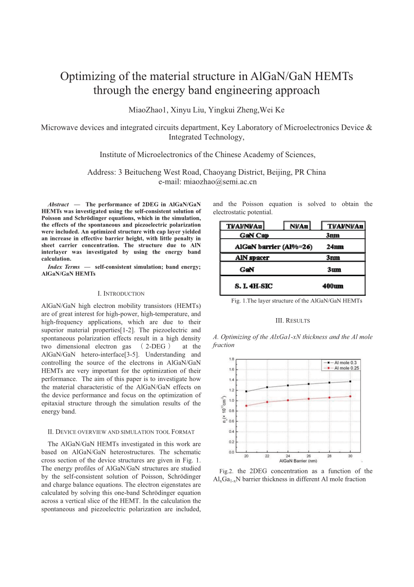
Pdf Optimizing Of The Material Structure In Algan Gan Hemts Through The Energy Band Engineering Approach
2
Www Systemplus Fr Wp Content Uploads 18 04 Sp165 Gan On Silicon Transistor Comparison Sample 3 Pdf
2

Barnstormer Hemt Prにて Hemtpr 来秋からジャケットなど セットアップ企画 Facebook

Hemt Pr サンプルセール 詳細になります ヘムト日記 平山洋次 Shop Brand Blog ショップ ブランドブログ Houyhnhnm フイナム
2
2

Device Characteristics Of Enhancement Mode Double Heterostructure Dh Hemt With Boron Doped Gan Gate Cap Layer For Full Bridge Inverter Circuit Mohanbabu 18 International Journal Of Numerical Modelling Electronic Networks Devices And
Http Www Diva Portal Org Smash Get Diva2 Fulltext01 Pdf
Http Www Nanoscience Gatech Edu Paper 1 S2 0 S Main Pdf
Electronics Free Full Text A Comprehensive Review Of Recent Progress On Gan High Electron Mobility Transistors Devices Fabrication And Reliability Html

Device Characteristics Of Enhancement Mode Double Heterostructure Dh Hemt With Boron Doped Gan Gate Cap Layer For Full Bridge Inverter Circuit Mohanbabu 18 International Journal Of Numerical Modelling Electronic Networks Devices And
Www Tu Ilmenau De Fileadmin Media It Hmt Vorlesungen Hft1 Hft1 Pdf
Ieeexplore Ieee Org Iel7 Pdf

Search Results For Rf Amplifier Rf Amplifier Datasheets Mouser Croatia
Http Www Jsts Org Html Journal Journal Files 19 12 Year19volume19 06 04 Pdf
2
Transfer Of Algan Gan Rf Devices Onto Diamond Substrates Via Van Der Waals Bonding
Http Www Jsts Org Html Journal Journal Files 19 12 Year19volume19 06 04 Pdf
Efficiency Improved By Monolithic Integration Of Hemt With Vertical Structure Leds And Mg Doping On Dry Etched Gan Journal Of Materials Chemistry C Rsc Publishing Doi 10 1039 C9tch
2
Pubs Acs Org Doi Pdf 10 1021 Acsami 7b
Electronics Free Full Text A Comprehensive Review Of Recent Progress On Gan High Electron Mobility Transistors Devices Fabrication And Reliability Html
Http Www Nanoscience Gatech Edu Paper 1 S2 0 S Main Pdf


